

94V0 High Quality Electronic Circuit Printing for Consumer Electronics
-
Price:
Negotiable
- minimum:
- Total supply:
-
Delivery term:
The date of payment from buyers deliver within days
-
seat:
Guangdong
-
Validity to:
Long-term effective
-
Last update:
2017-07-05 02:13
-
Browse the number:
282
+
Guangzhou NOD Electronics Co., Ltd.
- Contactaixin:
Mr. Rocky Long(Mr.)
-
Email:
telephone:
phone:

-
Arrea:
Guangdong
Address:Block3, #20-8, Huanxi West Rd, Tianhe District, Guangzhou, Guangdong, China 510660
- Website:
+
94V0 High Quality Electronic Circuit Printing for Consumer Electronics
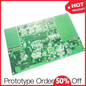
Products Display :

Professional Circuit Printing Manufacturing Capabilities
Our PCBA circuit printing manufacturing capabilities can meet high restrict technical requirements and cover almost 95% demand of customer requirements. In fact, we concentrated on this field for decades, so plant facilities have been advanced to high level and your intelligent manufacturing could be well handled here.
Circuit Printing Manufacturing Process

We are offering PCB circuit printing manufacturing and assembly services to following big customers all over the world

Trade Terms:
1. Payment: T/T in advance (Western Union , payple is welcomed)
2. Production lead time 100PCS: 5-7days, 500~1000PCS: 7-10days, above 1000PCS 15-20days.
3. Sample can be delivered in 3days
4. Shipping freight are quoted under your requests
5. Shipping port: Guangzhou, Huangpu,China
6. Discounts are offered based on order quantities
7. MOQ: 1PCS
If you have any other questions, welcome to contact us any time.
Products Display :
Professional Circuit Printing Manufacturing Capabilities
Our PCBA circuit printing manufacturing capabilities can meet high restrict technical requirements and cover almost 95% demand of customer requirements. In fact, we concentrated on this field for decades, so plant facilities have been advanced to high level and your intelligent manufacturing could be well handled here.
| Total Pad Size | Standard | Advanced |
| Capture Pad | Drill + 0.008 | Drill + 0.006 |
| Landing Pad | Drill + 0.008 | Drill + 0.006 |
| BC Mechanical Drill (Type III) | 0.008 | 0.006 |
| Laser Drill Size | 0.004-0.010 | 0.0025 |
| Material Thickness | 0.0035 | 0.0025 |
| Stacked Via | Yes | Yes |
| Type I Capabilities single & Double Deep | Yes | Yes |
| Type II Capabilities Buried Vias with Microvias | Yes | Yes |
| Type III Capabilities | Yes | Yes |
| Copper Filled Microvia | Yes | Yes |
| Smallest Copper Filled Microvia | 0.004 | 0.0025 |
| Copper Filled Microvia Aspect Ratio | 0.75:1 | 1:01 |
| Smallest Laser Microvia Hole Size | 0.004 | 0.0025 |
| Laser Via Aspect Ratio (Depth:Diameter) | 0.75:1 | c |
Circuit Printing Manufacturing Process
We are offering PCB circuit printing manufacturing and assembly services to following big customers all over the world
Trade Terms:
1. Payment: T/T in advance (Western Union , payple is welcomed)
2. Production lead time 100PCS: 5-7days, 500~1000PCS: 7-10days, above 1000PCS 15-20days.
3. Sample can be delivered in 3days
4. Shipping freight are quoted under your requests
5. Shipping port: Guangzhou, Huangpu,China
6. Discounts are offered based on order quantities
7. MOQ: 1PCS
If you have any other questions, welcome to contact us any time.
other products